https://insoobaik.tistory.com/660
SRAM 구조 및 동작 원리
보호되어 있는 글입니다. 내용을 보시려면 비밀번호를 입력하세요.
insoobaik.tistory.com
SRAM에 대한 내용은 위 글을 참고한다.
■ SRAM
SRAM은 기본적으로 clock, cs, we, ad, din, dout Pin을 가지게 된다.
- clock : 동기화를 위해 사용된다.
- cs : Chip Select로 해당 칩을 동작 시킬것인지 정하게 된다. High 신호에 동작하는 경우, cs가 1(High)일 때 만 Read, Write 행위가 가능하다.
- we : Write Enable로 해당 메모리에 Read할 것인지 Write할 것인지 정하게 된다 (ex we 신호가 0일 경우 Read, we 신호가 1일 경우 Write)
- ad : Address로 해당 메모리의 주소를 의미한다. (예를들어 64x8 SRAM이 있다면 6비트를 이용하여 해당 64개의 메모리 중 어떤 주소에 접근할 것인지 정하게 된다.
- din : Data In으로 메모리에 전달하는 Data에 해당한다.
- dout : Data Out으로 메모리에서 전달되는 Data에 해당한다.
■ 전체 코드
sram_model.sv
`timescale 1ns / 1ps

`define ASIC;

module sram_model #(
	parameter	DEPTH=8,
	parameter	WIDTH=32,
	parameter	DEPTH_LOG=$clog2(DEPTH)
)(
	input					clk,
	input					cs, we,
	input 	[DEPTH_LOG-1:0] ad,
	input 		[WIDTH-1:0]	din,
	output reg  [WIDTH-1:0]	dout
);
	reg [WIDTH-1:0]	mem[DEPTH-1:0];

	initial begin
		for (int i=0;i<DEPTH;i++)	mem[i] = 0;
	end

	always @(posedge clk)
		if (cs & we)	mem[ad]	<= din;
		else if (cs)	dout	<= mem[ad];
endmodule

module sram_fpga_64x8 (
	input					clk,
	input					cs, we,
	input 	[5:0] ad,
	input 		[7:0]	din,
	output reg  [7:0]	dout
);
	reg [7:0]	mem[63:0];

	initial begin
		for (int i=0;i<64;i++)	mem[i] = 0;
	end

	always @(posedge clk)
		if (cs & we)	mem[ad]	<= din;
		else if (cs)	dout	<= mem[ad];
endmodule

module sram_asic_64x8 (
	input					clk,
	input					cs, we,
	input 	[5:0] ad,
	input 		[7:0]	din,
	output reg  [7:0]	dout
);
	reg [7:0]	mem[63:0];

	initial begin
		for (int i=0;i<64;i++)	mem[i] = 0;
	end

	always @(posedge clk)
		if (cs & we)	mem[ad]	<= din;
		else if (cs)	dout	<= mem[ad];
endmodule


module sram_wrapper_64x8 #(
	parameter	DEPTH=8,
	parameter	WIDTH=32,
	parameter	DEPTH_LOG=$clog2(DEPTH)
)(

	input					clk,
	input					cs, we,
	input 	[DEPTH_LOG-1:0] ad,
	input 		[WIDTH-1:0]	din,
	output reg  [WIDTH-1:0]	dout
);
`ifdef SIM
	sram_model #(32, 8) 	u_sram (clk, cs, we, ad, din, dout);
`elsif FPGA
	sram_fpga_64x8 		u_sram (clk, cs, we, ad, din, dout);
`else
	sram_asic_64x8 		u_sram (clk, cs, we, ad, din, dout);
`endif
endmodule
전체 코드는 위와 같고, 핵심이 되는 코드는 아래와 같다.
	always @(posedge clk)
		if (cs & we)	mem[ad]	<= din;
		else if (cs)	dout	<= mem[ad];
clk 동기화에 맞춰 cs 1와 we 1 신호에 맞게 mem에 값을 Write하거나, cs 1 we 0 신호에 맞게 mem에 있는 Data를 읽어오도록 구성한 코드다.
■ `ifdef
위 코드를 보게 되면 `ifdef를 사용한 것을 확인할 수 있다.
`ifdef를 사용하는 이유는 RTL 설계시 FPGA, ASIC에 맞게 최적화된 코드가 서로 다를 수 있다.
상위 모듈(위 코드에선 wrapper) 기준으로 하위 모듈을 생성하게 되면 필요한 상황에 맞게 유연하게 코드를 관리할 수 있다는 장점이 있다.
`define FPGA;

...
...
...

module sram_wrapper_64x8 #(
	parameter	DEPTH=8,
	parameter	WIDTH=32,
	parameter	DEPTH_LOG=$clog2(DEPTH)
)(

	input					clk,
	input					cs, we,
	input 	[DEPTH_LOG-1:0] ad,
	input 		[WIDTH-1:0]	din,
	output reg  [WIDTH-1:0]	dout
);
`ifdef SIM
	sram_model #(32, 8) 	u_sram (clk, cs, we, ad, din, dout);
`elsif FPGA
	sram_fpga_64x8 		u_sram (clk, cs, we, ad, din, dout);
`else
	sram_asic_64x8 		u_sram (clk, cs, we, ad, din, dout);
`endif
endmodule
`ifdef는 특정 조건이 만족될 때만 호출하게 된다.
위 코드의 경우 SIM, FPGA, 그외 값이 정의되면 module을 생성하도록 정의되어 있으며 코드 가장 위를 보게 되면 `define으로 FPGA가 정의되어 있는 것을 볼 수 있다. 위에 생략된 부분에 sram_fpga_64x8 module이 정의되어 있으며, wrapper 상위 모듈의 하위 모듈로 FPGA 최적화 코드를 사용하게 되는 것을 알 수 있다.
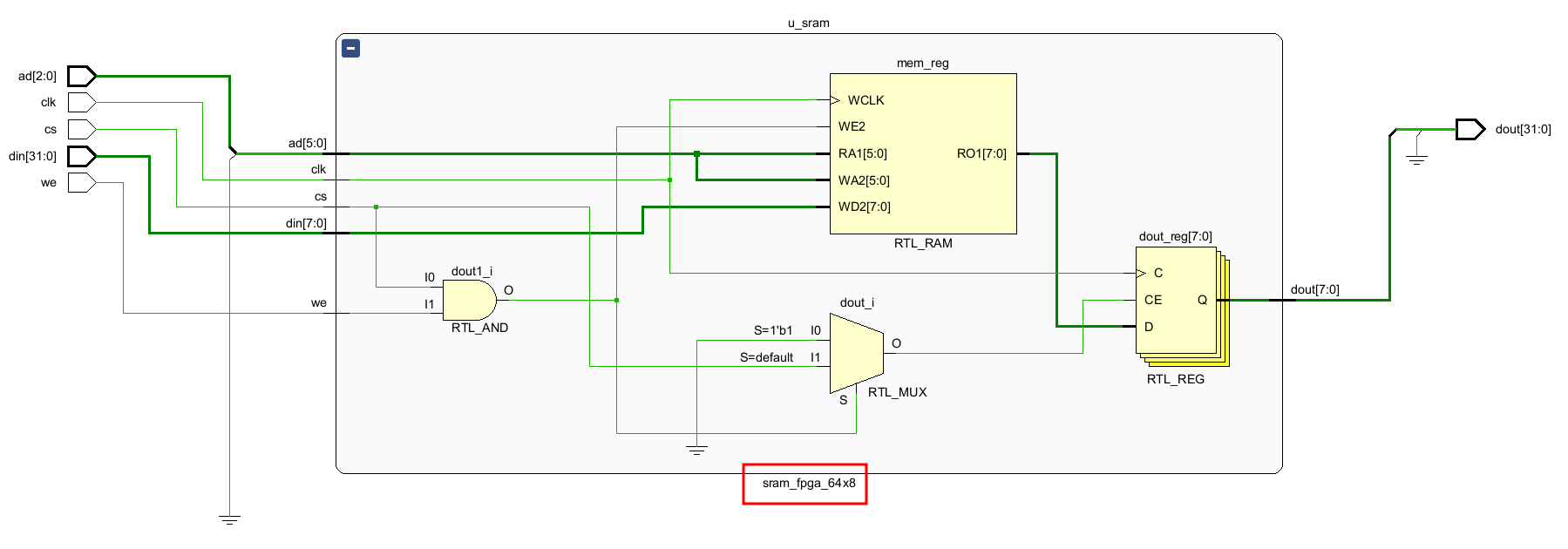
`define FPGA를 사용했을 때 Schematic
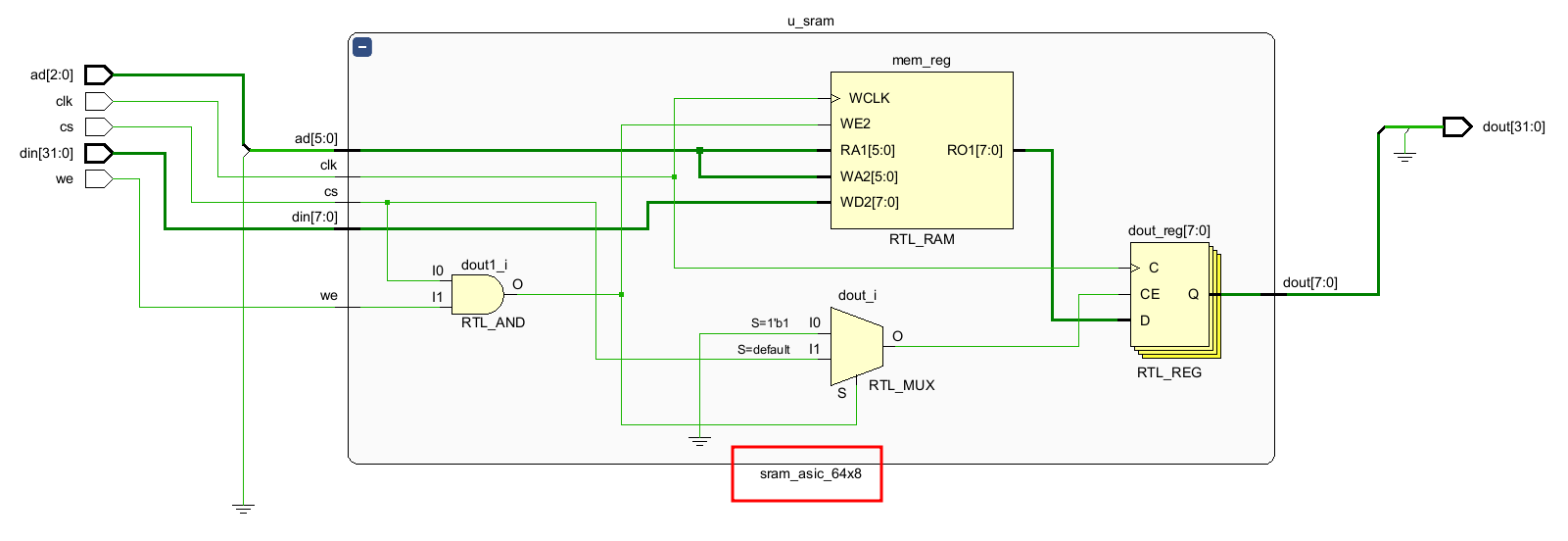
`define 그 외(ASIC)를 사용했을 때 Schematic
■ Test bench & Simulation
WRITE
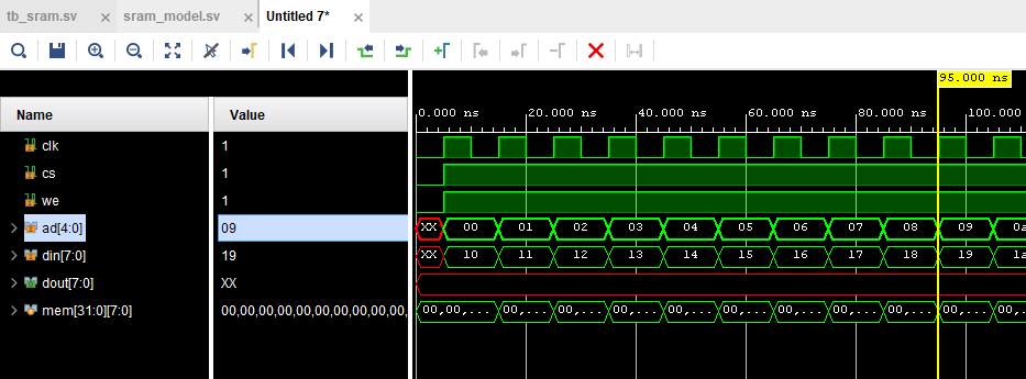
cs == 1 (동작) & we == 1 (WRITE) 일 때 din을 통해 mem에 값이 저장되는 것을 확인할 수 있다.
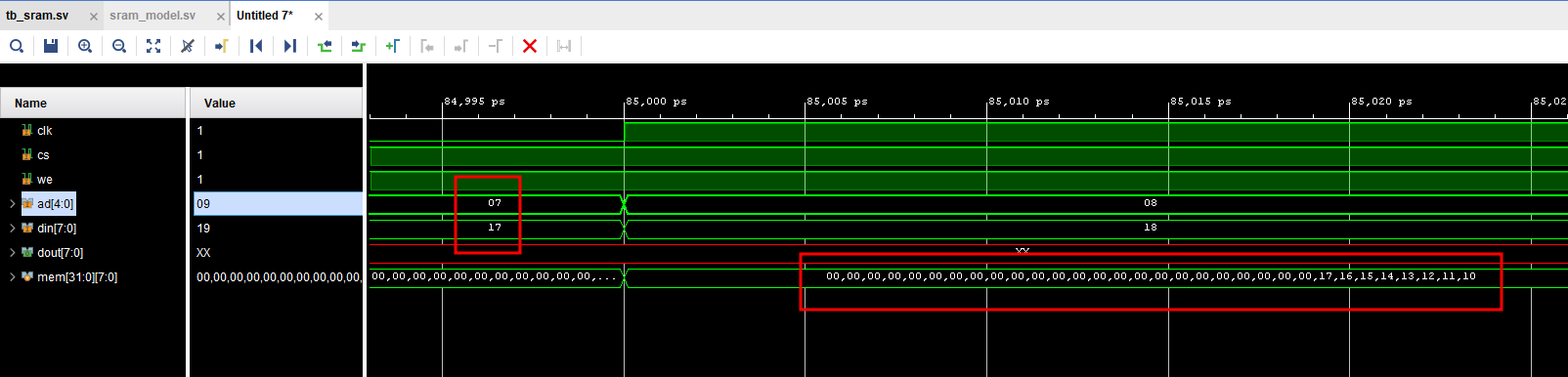
READ
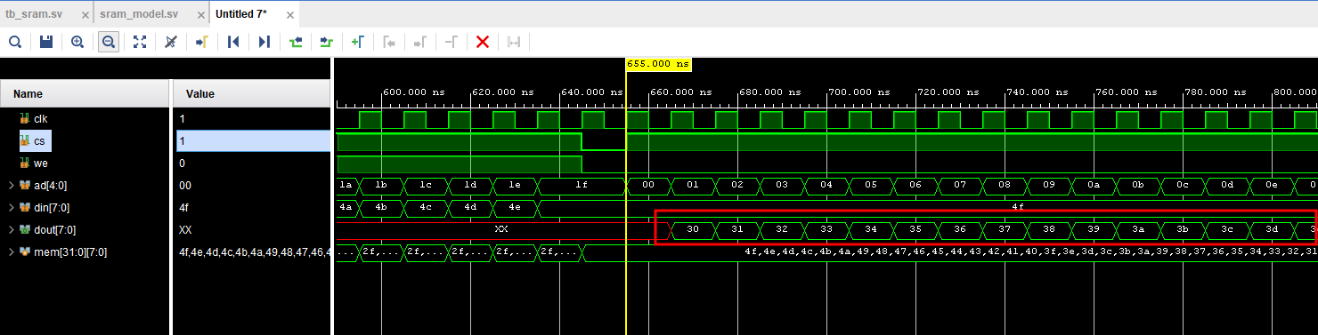
cs == 1 (동작) & we == 0 (READ) 일 때 mem의 ad에 해당하는 부분의 DATA가 dout을 통해 출력되는 것을 확인할 수 있다.
'Semiconductor > RTL, Simulation' 카테고리의 다른 글
| RTL - Two Port SRAM / Dual Port SRAM 구조 및 설계 (0) | 2024.08.07 |
|---|---|
| RTL - CACHE(Two Port SRAM) 동작 과정 및 설명 (0) | 2024.08.07 |
| RTL - SPI (Master, Slave, FSM) (2) FSM, MASTER, SLAVE & SLVAE 활용 (0) | 2024.06.02 |
| RTL - SPI (Master, Slave, FSM) (1) FSM, SLAVE (0) | 2024.06.02 |
| RTL - Xcelium, Verilog를 이용한 CPU RISC 구조 설계 (0) | 2024.06.02 |